**The AD7828KP: A Comprehensive Guide to Maximizing Performance in High-Speed Data Acquisition Systems**
In the realm of high-speed data acquisition (DAQ), the performance of each component is critical to the integrity of the entire system. The **AD7828KP**, an 8-bit, 8-channel analog-to-digital converter (ADC) from Analog Devices, stands as a pivotal component designed for such demanding applications. Achieving its maximum potential, however, requires a deep understanding of its architecture and a meticulous approach to system design. This guide outlines the key strategies for optimizing the performance of the AD7828KP.
**Understanding the Core Architecture**
The AD7828KP integrates eight 8-bit ADCs with a **high-speed parallel interface**, capable of a 2 MSPS aggregate sampling rate. Its success hinges on a half-flash (or subranging) conversion technique, which balances speed with power efficiency. Each channel can be sequentially sampled, making it ideal for multi-point monitoring systems where space and component count are constraints. The internal track-and-hold amplifier is fundamental to capturing fast-changing signals accurately.
**Critical Design Considerations for Maximum Performance**
1. **Power Supply and Decoupling:**
A clean and stable power supply is non-negotiable. **Bypass capacitors** are your first line of defense against noise. Employ a combination of bulk (10µF), ceramic (0.1µF), and high-frequency (1-10nF) capacitors placed as close as possible to the `VCC` and `VDRIVE` pins. A low-noise, linear regulator is strongly recommended over a switching type to prevent introducing high-frequency noise onto the supply rails.
2. **Reference Voltage (VREF) Stability:**
The accuracy of any ADC is directly tied to the stability of its reference voltage. The internal reference of the AD7828KP is sufficient for many applications, but for ultimate performance, consider buffering it or using an **external, low-noise reference** source. Ensure the reference input is heavily decoupled to ground to minimize noise.
3. **PCB Layout and Grounding:**
**Proper grounding is arguably the most critical factor** in high-speed design. Utilize a ground plane to provide a low-inductance return path for currents. Partition the board into analog and digital sections, placing the AD7828KP at the boundary. All analog inputs and the reference should run over the analog ground plane, while digital outputs should be routed over the digital plane. This minimizes digital noise corrupting sensitive analog signals.
4. **Managing the Digital Interface:**
The high-speed parallel data output can generate significant transient currents. To isolate the ADC's digital noise from its analog core, use the `VDRIVE` pin to match the digital output logic levels to the host system (e.g., 3.3V or 5V). **Employ buffering latches or FIFO memory** immediately at the digital outputs of the ADC to capture data. This prevents noisy digital lines from running back near the analog inputs and allows the host microcontroller to read data at its own pace.
5. **Signal Conditioning and Anti-Aliasing:**
The analog input path must be pristine. For dynamic signals, a dedicated **operational amplifier driver** should be used to provide a low-impedance source and isolate the signal from the ADC's switching inputs. Furthermore, an **anti-aliasing filter (AAF)** is mandatory. For a 2 MSPS system, a simple passive RC low-pass filter with a cutoff frequency just above your signal of interest will effectively reject out-of-band noise and prevent aliasing.
6. **Clock Integrity:**
The conversion process is initiated by the `CONVST` (Convert Start) pulse. This signal must be clean and jitter-free. **Clock jitter directly degrades the Signal-to-Noise Ratio (SNR)** of the sampled data, especially for higher-frequency input signals. Use a stable oscillator and route the `CONVST` signal as a controlled-impedance trace, away from analog input lines.
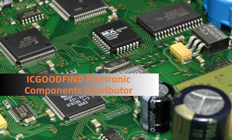
**ICGOOODFIND**
The AD7828KP remains a highly capable ADC for multi-channel, medium-resolution, high-speed applications. Maximizing its performance is not just about the chip itself but about the entire ecosystem surrounding it. By focusing on impeccable power integrity, rigorous PCB layout, intelligent interface management, and robust signal conditioning, engineers can unlock the full potential of this converter, ensuring data acquisition systems perform with exceptional accuracy and reliability.
**Keywords:** High-Speed Data Acquisition, Anti-Aliasing Filter, PCB Layout, Reference Voltage Stability, Signal Conditioning